For this project, we're going
to make a block for the octave shifter and then create an overall
schematic that has only three blocks in it. This will make things less
confusing as we add still more circuitry to the tone translator. It's
like we're creating three custom integrated circuits to do the jobs of
the timing signal circuit, the up-counter circuit, and the octave
shifter circuit.
- Get into Windows Explorer and make a folder called gj09_18_three_blocks.
- Copy
the following files into the folder you just created (these are files
from previous experiments, and yours may have slightly different names):
- gi21_13_tone_translator_up_counter.sch
- gj01_10_timing_signals_improved.sch
- gj05_09_octave_shifter_and_blocks.sch
- gj05_09_octave_shifter_and_blocks.abv
- Make a copy of gj05_09_octave_shifter_and_blocks.sch and rename the copy gj05_09_octave_shifter_block.sch.
- Change the name of gj05_09_octave_shifter_and_blocks.sch to gj09_18_three_blocks.sch.
- This is going to be our top-level schematic and will eventually only have three blocks in it.
- Change the name of gj05_09_octave_shifter_and_blocks.abv to gj09_18_three_blocks.abv
- Get
into Lever and create a new project called gj09_18_three_blocks, and
select the gj09_18_three_blocks folder as the folder where all the
files will go.
- As we've been doing, use the Lever default device.
- Import all four schematic files into the project.
- For each schematic file, generate a schematic symbol.
- In the Sources in Project window, click on one of the schematic files.
- In the Processes for Current Source window, double-click Generate Schematic Symbol.
- Click Window, Library Manager to open the library manager.
- In the Library Manager window, click File, Open Folder.
- Click the gj09_18_three_blocks folder, and then click OK.
- In
the window that comes up, you should see the names of the four
schematic files you've imported. They're now part of the local library.
- Close the library manager window.
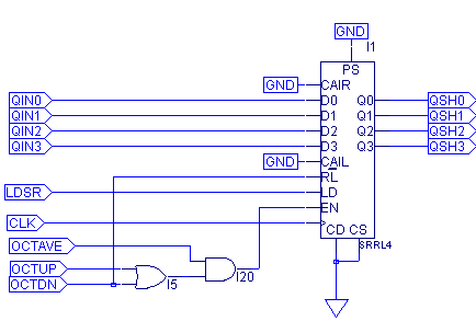
- Double-click the octave shifter file (in the Sources in Project window) to open it up into the schematic editor.
- We're going to make the shift register and it's two
gates into a new block. To do this, we're going to delete everything
except the octave shifter part of the circuit. Start by deleting the
following:
- The gj01_10_timing_signals_improved block
- The gi21_13_tone_translator_up_counter block
- The PERIOD_IN input pin and the wires connected to it.
- The following output pins and their associated wires: PERIOD_IN, TS_CD, TS_CAI, TS0, TS1, TS2, TS3, TS4, INCNT, LDOUTCNT, OUTCNT, CYCLE_END, PERIOD_IN_SYNCD, and IN_CNT_CAI.
- You'll probably be left with a wire stub all by itself labeled CLK. Delete it (but don't delete the CLK input pin)
- The shift register is the only place where CLK is used in this schematic.
- Delete any bits of wire that used to go somewhere, but now don't.
- Connect the CLK input pin to the shift-register's clock input.
- Change the following output pins to input pins:
- LDSR
- OCTAVE
- QIN0
- QIN1
- QIN2
- QIN3
- For
each of these new input pins, select it with the Move tool and then
press CTRL R two times. This should rotate it 180 degrees.
- Fix up any wiring problems created by rotating the pins.
- You should now have a schematic like that shown below.
- Click File, Matching symbol. If the computer asks if you want to replace the existing file, say yes.
- Click DRC, Consistency Check (and if there are errors, fix them).
- Click File, Save.
- In the project navigator window, double-click the gj09_18_three_blocks.sch file to open it into the schematic editor. You'll probably see Schematic Editor flashing in orange at the bottom of your screen. Click it to bring up the schematic editor window.
- If you don't have plenty of extra space on the "page", click File, Sheets, Resize and then choose the D-size paper.
- Delete the shift register and the two gates associated with it, but don't delete any input or output pins.
- We're going to replace the shift register and the two gates with the octave shifter block we just created.
- Select the Add Symbol tool from the tool box. Be sure [Local] is the library selected in the top window.
- In the bottom window, choose gj05_09_octave_shifter_block.
- Place the block somewhere on the schematic where there's room.
- Move the OSH output pins over so that the octave shifter block will fit.
- To the octave shifter block, connect all the wires it needs.
- You shouldn't need to create any new input or output pins.
- You should now have a schematic that looks similar to the one at the top of this Web page.
- Click File, Matching Symbol.
- Click File, Save
- Close the schematic editor.
- In the project navigator's Sources in Project window, be sure gj09_18_three_blocks is highlighted.
- Double-click Compile Schematic.
- Import the test vector file you copied into the folder at the beginning of these procedure steps, and compile it.
- Double-click Functional Simulation, and compare your waveforms to the ones near the top of this Web page.
|