This project uses only gates and
inverters (no flip-flops, etc.). The combinatorial circuit you
design will be similar to one we'll be designing in a future
tone-translator lab project to determine what musical note has been
picked up by the microphone. (This note determining circuit will
be taking seven outputs from a counter and then making one of 12
outputs go high, corresponding to the notes C, C#, D, D#, E, F, F#, G,
G#, A, A#, B.)
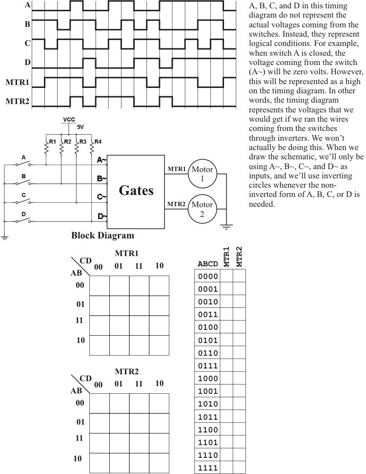
In the block diagram below, the rectangle represents the combinatorial
circuit you'll be designing. This block has inputs from four switches
and it produces two outputs (one for Motor 1 and one for Motor 2).
Here is the procedure to follow for designing the combinatorial circuit
for the current project:
- Refer to the example for this project. (It's a handout
sheet and isn't on this Web site.)
- The four inputs to your circuit are A~, B~, C~, and D~
(representing A not, B not, C not, and D not) .
- As with most digital circuits involving switches, closing
a switch grounds a line connected to a pull-up resistor. Thus, the
wires coming from switches A, B, C, and D provide the logic
variables A~, B~, C~, and D~ (rather than A, B, C, and D).
- Don't worry about the fact that you only have the
complements available to work with. As you're working on the design in
the following steps, think in terms of A, B, C, and D (rather thanA~,
B~, C~, and D~
). When you get to the step where you draw gates, simply use an
inverting circle wherever you need the non-complemented form of an
input.
- Above each column of the timing diagram, write the binary
number for ABCD, with A being the most significant bit.
- For example, the number for the first two columns are
0110 and 0100.
- Fill in the MTR1 and MTR2 columns of the truth table.
- For MTR1, notice that there are only 5 places where the
signal goes low. Thus, the easiest way to fill in the truth table for
this signal is to write zeroes in the rows where MTR1 is low. Then,
simply write ones in the places that don't contain zeroes.
- For MTR2, notice that there are only 5 places where the
signal goes high.
- Convert the truth table into Karnaugh maps for MTR1 and
MTR2.
- Draw circles around groups of ones in both maps. (We're
calling them circles, even though they are actually loops rather than
true circles.)
- You should have three circles on the MTR1 map. One of
these circles will be a simple circle, and the other two will be
wrap-around circles. For these wrap-around circles, you'll be drawing
half a circle in one place and the other half on the opposite side of
the map.
- You should have two wrap-around circles on the MTR2 map.
- On both maps, there will be places where some of the
circles overlap. (Remember, overlaps are desireable.)
- Write equations for both maps.
- For the MTR1 map, you should have three terms separated
by plus signs.
- For the MTR2 map, you should have two terms separated by
plus signs.
- On a piece of papter, draw gates to implement the MTR1
equation.
- Your circuit should only contain the four inputs A~,
B~, C~, and D~ (corresponding to lines coming from the four
switches).
- You should only need three gates.
- Use inverting circles rather than inverters.
- Draw gates to implement the MTR2 equation.
- You should be able to re-use the outputs from two of the
MTR1 gates. This will result in your only needing two gates for the
MTR2 circuit.
- Using Lever, draw the schematic (just the gates, not the
switches, pull-up resistors, and motors).
- Lever allows tildes ( ~ ), so use A~, B~, C~, and D~ as
the net names for the four inputs.
- Simulate the circuit to see if it produces a
timing diagram the same as the one below.
- For this project, you'll be creating your own test-vector
file rather than downloading one that's already made.
|