- Get into ispLever Project Navigator
- File, New Project
- Use gh27_13 as the project name
- At the right of the Location box is a button with three dots. Click this button.
- Find your folder (in My Documents, your floppy, or flash drive) and single-click it.
- Click the Make New Folder button.
- Name the new folder gh27_13.
- Press Enter (on the keyboard) and then click OK.
- In the Design Entry Type box, choose Schematic/VHDL
- Click Next
- In the Family box, choose ispLever Default Device.
- Click Next.
- When the Add Source window comes up, click Next.
- Click Finish.
- Click Window, Schematic Editor (on the menu bar).
- There should be a window within the window that opens, and it should be named Drawing. This is the Drawing Toolbar.
- If there is no Drawing Toolbar, click View, Drawing Toolbar.
- In the Drawing Toolbar, click the AND gate icon in the upper left-hand corner. This is the Add Symbol tool.
- In the remaining steps, toolbar means the Drawing Toolbar (unless otherwise stated).
- In the Library box, click the line that contains the word generic.
- Click and2.
- In the drawing area, click the mouse to place the AND gate in your drawing.
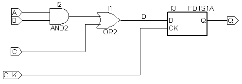
- Do the same to place an OR gate (or2) and a D flip-flop (FD1S1A).
- Click the Move tool (the four-headed arrow in the center of the drawing toolbar).
- Click the plus magnifying glass on the main toolbar.
- Draw a box around the three symbols.
- Move the gates and the flip-flop into the positions shown in the schematic at the top of this Web page.
- To use the Move tool, first click the object you want to move and then release the mouse button. You may then move the object to the desired position.
- Click the Add wire tool.
- Wire up the components.
- Once you get to the end of a wire, do a right-click to break off the wire.
- Add short wires onto the two AND gate inputs and onto the lower OR gate input. Also, add a short wire to the Q output of the flip-flop.
- This is necessary because of a quirk in the schematic editor: You can't add IO connectors directly to the leads coming out of a component.
- Click the Add Net Name tool (second one down in the middle toolbar column).
- Type A in the lower left-hand corner of the screen, and press Enter.
- Put the center of the crosshairs directly over the red box on the end of the wire coming from the top input of the AND gate.
- Do the same to add the net names LFXP10C-5F388C.
- For net name D, use the same procedure, except put the crosshairs on the blue line going between the OR gate and the flip-flop.
- Click the I/O marker tool (second one down in the right toolbar column).
- The window that comes up should already have Input selected.
- Draw a box around net names A, B, C, and CLK.
- Choose Output in the I/O box.
- Draw a box around net name Q.
- Click File, Save As (in the menu bar).
- Be sure gh27_13 appears in the Save in box.
- Put gh27_13 in the File name box.
- In Project Navigator, highlight LFXP10C-5F388C in the Sources in Project window.
- Click Source, Import (menu bar).
- Double click gh27_13 (which is the schematic file you just saved).
- Below LFXP10C-5F388C, you should now see [gh27_13(gh27_13.sch)].
- That's all for this project. For the next project, we'll use this schematic file to create the programming for the PLD (programmable logic device).